
- Round draws state-backed funds and rare participation from China’s national social security fund
- Deal highlights shift from tool substitution to full-stack chip design software capabilities
Shanghai Leda Technology (立芯科技) has raised more than 300 million yuan ($44 million) in a Series C round, with participation from a mix of state-backed investors, venture capital firms and a rare investment from China’s national social security fund.
The round was led by Cowin Partners, Haiwang Capital together with Shenzhen Capital Group, China Internet Investment Fund and Fujian Electronics.
The social security fund’s participation is being viewed by industry observers as a signal that domestic digital electronic design automation (EDA) tools have moved beyond validation and into engineering-scale deployment.
Potential chokepoint
EDA, often described as the “mother of chips,” underpins chip design, manufacturing and packaging workflows. The sector has long been dominated by Synopsys, Cadence and Siemens EDA, which together account for roughly 74% of global market share.
The global EDA market is projected to reach $18.3 billion by 2026, while China’s domestic market is expected to hit 222 billion yuan, growing faster than the global average as localization accelerates.
The push for domestic alternatives is driven by concerns over supply-chain vulnerability, with EDA tools seen as a potential chokepoint in China’s semiconductor ecosystem if external access is restricted.
At the same time, industrial policy emphasis has increasingly focused on ensuring resilience under extreme scenarios, reinforcing the need for self-sufficiency in core design infrastructure.
Pivot to full-process platforms
Industry development is shifting from point-tool replacement toward full-process platforms, with increasing emphasis on DTCO (design-technology co-optimization) and STCO (system-technology co-optimization) methodologies.
Huawei’s Tau Scaling Law, often cited in industry discussions, reflects a broader post-Moore’s Law transition from physical scaling to system-level efficiency and timing optimization.
However, manufacturing-stage EDA remains the weakest link in China’s stack, with localization still below 10%, making it a priority area for further development.

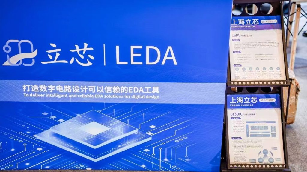
Founded in 2020, Leda develops digital circuit physical design, logic synthesis and 3D IC/Chiplet system-level design tools.
Its product suite includes LeDI, LePV, LePI and Le3DIC, and serves more than 60 fabless companies and foundries, supporting domestic advanced-node development and verification.
A Fudan-incubated startup
The company is now shifting toward a full-stack “agentic EDA” architecture, centered on its LeBrain system and two AI agents, LeDSE and LeDesigner, forming a closed loop covering perception, decision-making, execution and verification.
Founder Chen Jianli is a professor at Fudan University’s School of Microelectronics and a doctoral supervisor. His team won the DAC best paper award in 2017 — the first time researchers from mainland China achieved the honor as a first-author institution in the conference’s 54-year history.